What do a meniscus, actinic radiation, and highly precise injection molded optical elements have in common? They come together in a newly patented process for molding micro-optics authored by a pair of IBM employees.
August 12, 2013
What do a meniscus, actinic radiation, and highly precise injection molded optical elements have in common? They come together in a newly patented process for molding micro-optics authored by a pair of IBM employees.
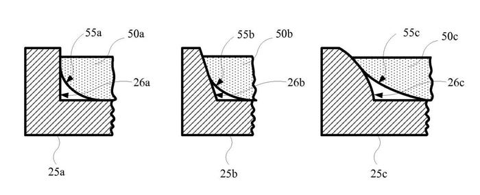
The patent, entitled "Spin-mounted fabrication of injection molded micro-optics" was filed in May 2012 and published in July 2013. The technology is described as designing the mold cavities with a curved shape approximately corresponding to an optical profile. Then the melt is injected, it forms what the patent calls a "meniscus" due to the material freezing off and surface tension between the melt and the cavity wall. As the patent states, "the meniscus thus provides a shape corresponding to the predetermined optical profile," with the material then rapidly cured via actinic radiation, an electromagnetic form of radiation that can produce photochemical reactions. The result:
"A desired optical element with high-precision dimensions is formed within the cavities of the moldplate."
The patent also describes an alternative process where "the moldplate is spun such that the meniscus is adjusted to match the predetermined optical profile within a certain tolerance."
The technology, described by IBM's Casimer M. DeCusatis and Lawrence Jacobowitz, was issued U.S. patent No. 8485812.

Micro-optic patent
About the Author(s)
You May Also Like


