Laser Technology Optimizes Joining of Micrometer-Sized Transparent Plastic Parts
Developed by researchers at Germany’s Fraunhofer Institute for Laser Technology ILT in collaboration with industrial partners, the SeQuLas process has notable applications in the fabrication of micro-fluidic chips for medical devices.
July 21, 2020

A joining technique for transparent plastic parts powered by a thulium fiber laser does not require the use of absorbers because the laser’s wavelength aligns with the material’s natural absorption range. Developed by researchers at Germany’s Fraunhofer Institute for Laser Technology ILT in collaboration with industrial partners, the process has notable applications in micro-fluidic chips for medical applications.
The three-year SeQuLas project, which was successfully completed earlier this year, produces minute weld seams in transparent plastic components. This has been a challenge for conventional joining technologies, which reach an impasse in the micrometer range, a potential roadblock in the fabrication of micro-fluidic devices, explained Fraunhofer ILT.
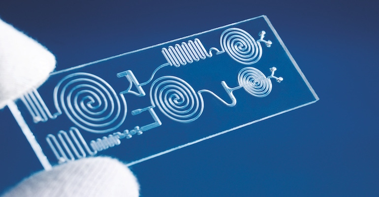
Micro-fluidic chips are designed to efficiently transport, mix, and filter small amounts of liquids. The devices enable lab-on-chip technology, by which chemical analyses can be performed, often based on a minute amount of blood, for the early detection of disease as well as patient monitoring. A major challenge in the fabrication of the devices, noted Fraunhofer ILT, is the extremely tight encapsulation of micro-channels in the chips. “Conventional joining technology reaches its limits in the micrometer range. In its place, absorber-free laser transmission welding — with beam sources in the near-infrared range — allows high precision and flexibility, making it the ideal solution,” said Fraunhofer ILT in a press release on its website.
The global microfluidic device market is forecast to reach a value of $22.6 billion by 2026, driven by a compound annual growth rate just above 20% from 2019 through the forecast period, according to Fortune Business Insights.
In the beginning
Fraunhofer ILT launched the SeQuLas project in 2017, in collaboration with Amtron GmbH, Ortmann Digitaltechnik GmbH, and Bartels Mikrotechnik GmbH. The project was funded through a regional development agency in the German state of North Rhine Westphalia along with the European Regional Development Fund.
SeQuLas stands for “segmental quasi-simultaneous laser irradiation,” which involves the use of a thulium fiber laser with an emission wavelength of 1940 nm as the beam source. This is the natural absorption range of plastics and eliminates the need to add absorber materials. Consequently, transparency of the chip is not affected during laser processing. However, absorber-free laser transmission welding creates its own challenge, which Fraunhofer ILT and its industrial partners overcame.
|
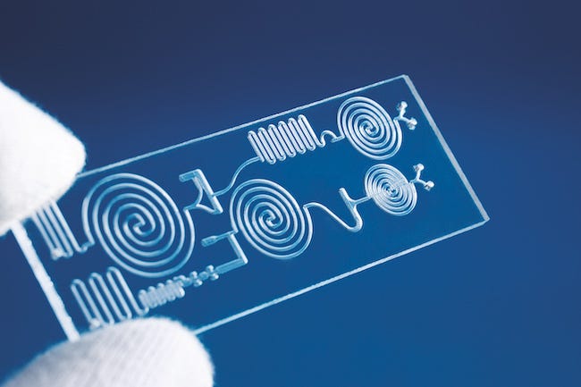
Micro-fluidic chips enable lab-on-chip technology, by which chemical analyses can be performed, often based on a minute amount of blood. Image courtesy Fraunhofer ILT. |
Volume absorption creates a heat-affected zone (HAZ) that extends vertically over the entire cross-section of the component, explained Fraunhofer ILT. Thermal expansion during the melting process may result in the formation of blowholes and cracks that cause leaks in the seam structure. Moreover, it may cause the material to warp, especially if flat components are being processed.
Researchers discovered that quasi-simultaneous irradiation could be used to reduce vertical expansion of the HAZ. In this process, a laser beam moves along the weld contour several times at high speed with the aid of a scanner system. The entire seam contour is heated simultaneously, instead of sequentially, as happens under contour welding. In tests with polycarbonate components, Fraunhofer ILT demonstrated that during the welding process the heat is dissipated at the outer surfaces while accumulating inside the material. Compared with contour welding, the process reduced vertical expansion of the HAZ by up to 30%.
Early detection of thermal damage
In a second step, the project partners developed a process control for the laser welding technology. A pyrometer integrated in the beam path measures the temperature in the component during the welding process. By coupling the measurement signal with the position of the scanner mirrors, thermal damage in the component can be recorded and precisely localized during the welding process. The newly developed welding process, therefore, can react quickly to temperature deviations and control the laser power accordingly. In this way, homogeneous seam properties along the seam contour can be ensured, said Fraunhofer ILT.
You May Also Like


