Sponsored By
News
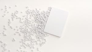
Polycarbonate resin with 90% PCR content 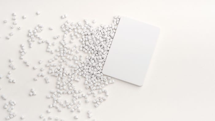
Automotive & MobilityCovestro Debuts Polycarbonate with 90% Recycled ContentCovestro Debuts Polycarbonate with 90% Recycled Content
The carbon footprint of the new material is 70% smaller than conventional virgin resin, yet can be used in demanding highly saturated color and flame-retardant applications.


 shuttle")


Editor's Choice

Sign up for the PlasticsToday NewsFeed newsletter.